list
- an Omicron variable temperature (15-900 K) ultrahigh vacuum (UHV) scanning tunneling microscope(STM)/atomic force microscope(AFM). This multifunction variable-temperature scanning probe microscope (VTSPM) is housed in a UHV chamber with various thin film growth and characterization facilities, such as mini-MBE, gas dosing train, load lock lines, sputtering gun, low-energy electron diffractometer, sample cleaving facility, atom source, and e-beam bombard facility etc;
- an Omicron room temperature STM/AFM housed in a UHV chamber with various thin-film growth and characterization facilities.
- an Omicron low temperature (4K) STM/AFM connected to the RT STM/AFM of (2), forming a powerful combined system for nanoscale and atomic level characterization of materials surfaces.
- an ambient AFM PSIA system, with additional capabilities to do STM, electric(magnetic) force imaging, and experiments in liquid.
- a home-built radio-frequency STM (RFSTM) system. The RFSTM is our patented technique (US patent US8863311). It can achieve a detection bandwidth thousands times more than conventional STM. It can also detect atomic features on surface in situ with external current or light (X-ray), enabling experiments not possible before (e.g., atomic chemical detection by STM).
- a well-equipped electronic shop for RFSTM development.
- a temperature programmed desorption system to study surface reaction kinetics.
- two chemical vapor deposition (CVD) systems for growth of superior quality functionalized graphene and other materials.
- there are couple systems that are functional but rarely used in the laboratory, including an Ibach high-resolution low energy electron energy loss (HR-EELS) system and a general UHV system.
To perform other experiments, the laboratory uses facilities at Taiwan’s synchrotron radiation sources and collaborates with groups with optical characterization (Raman etc.). The laboratory has foreign collaboration projects with groups in France, Russia, and Israel.
In addition, our laboratory is handy in developing new methods of surface characterization and possesses capability to build tools beyond commercial reach.
In the following, more details of the above listed items are described.
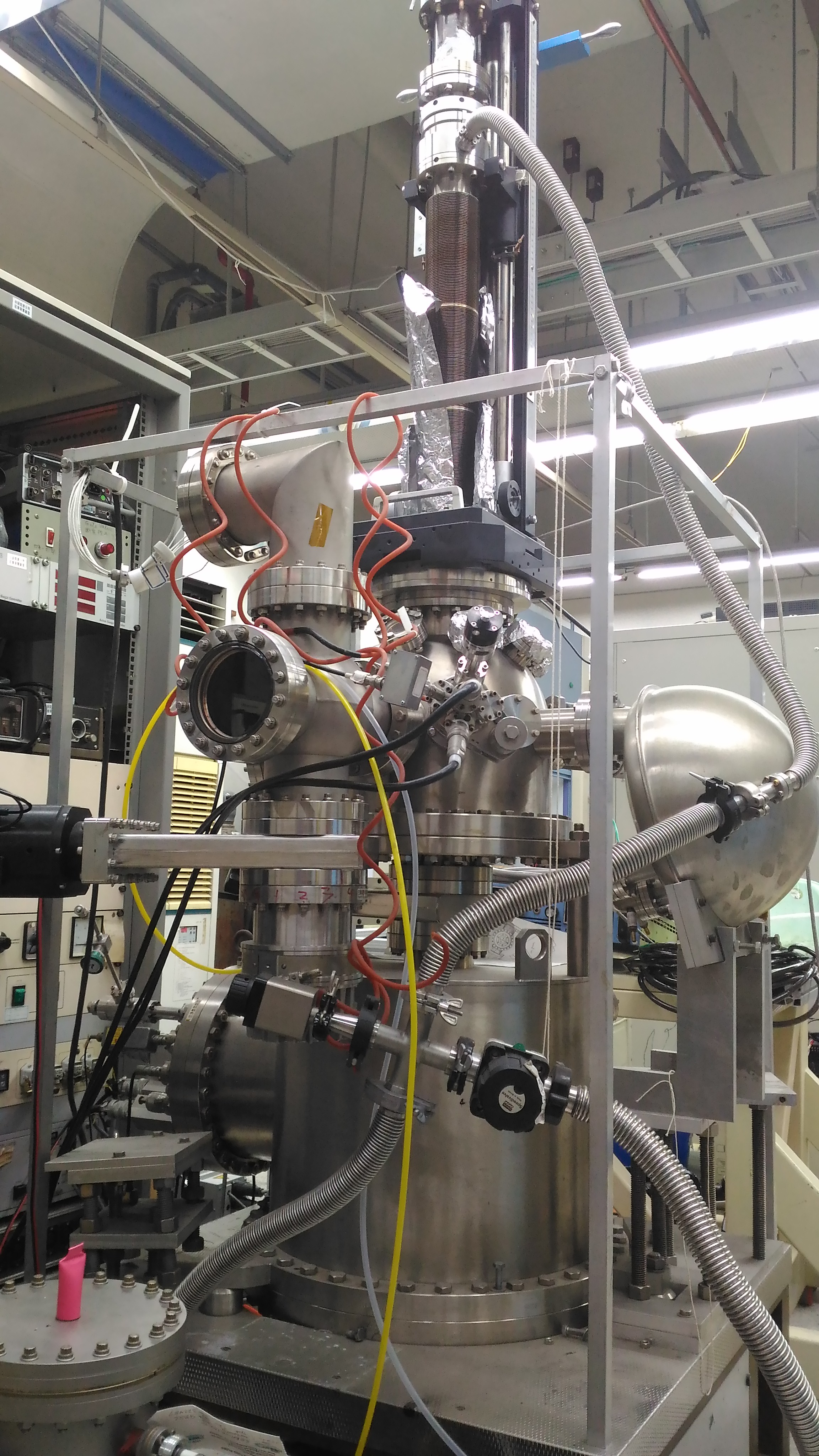
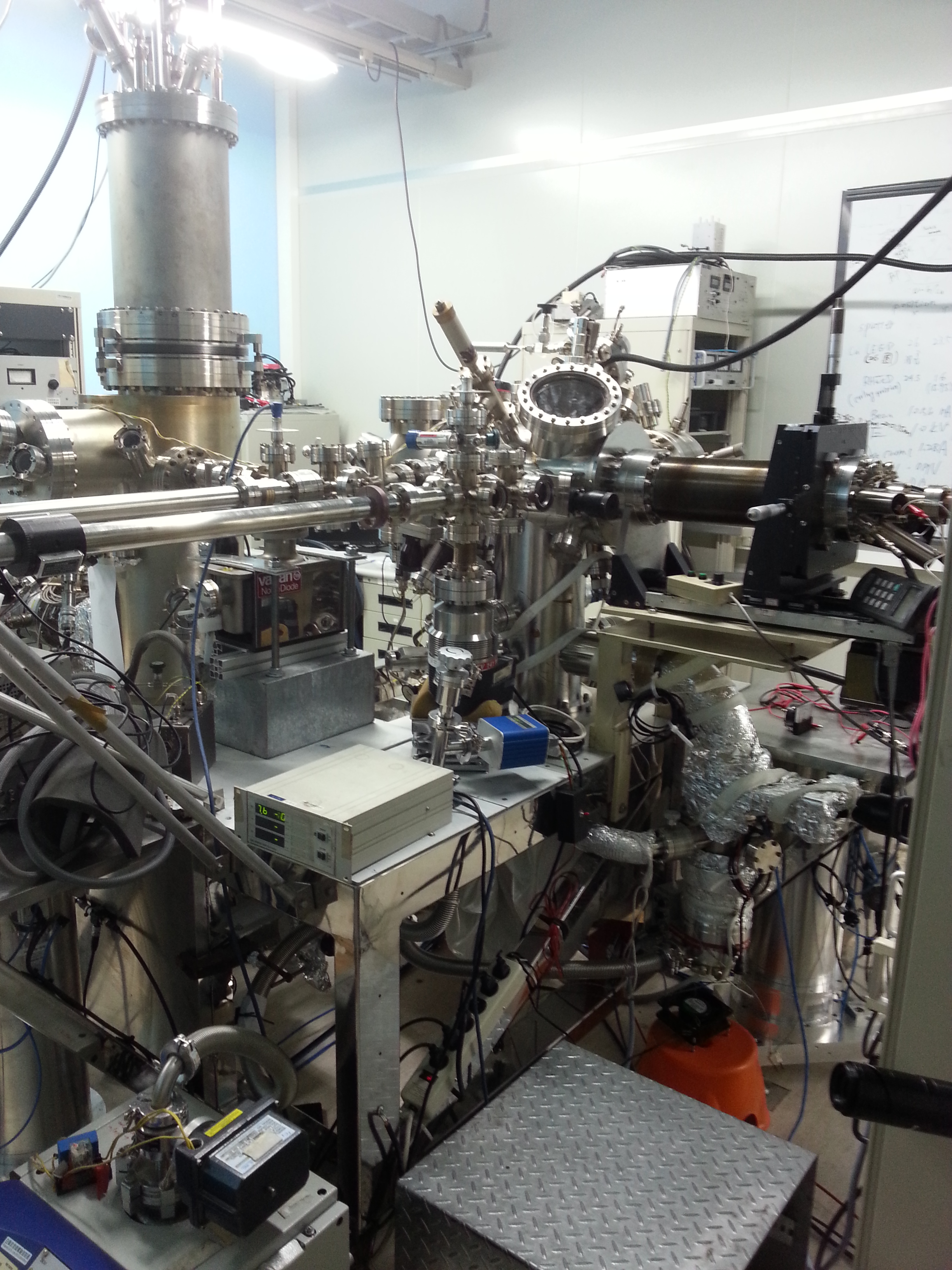
(1) Omicron variable-temperature STM/AFM system (15-900 K)
This system can perform scanning tunneling microscopy, non-contact atomic force microscopy and other multi-modes operations. The accessible range of sample temperature is from 15 K to 900 K. With high-magnification optical aid, samples of micron sizes can be studied. The pressure is lower than 5 x 10-11 Torr. The system is equipped with a 4-grid reverse LEED/Auger, K-cell, mini MBE, radical cracker source, gas train, load lock systems, residual gas analyzer, sample cleaver, LN2-cooled manipulator, focused sputtering gun and tip bombard heater.
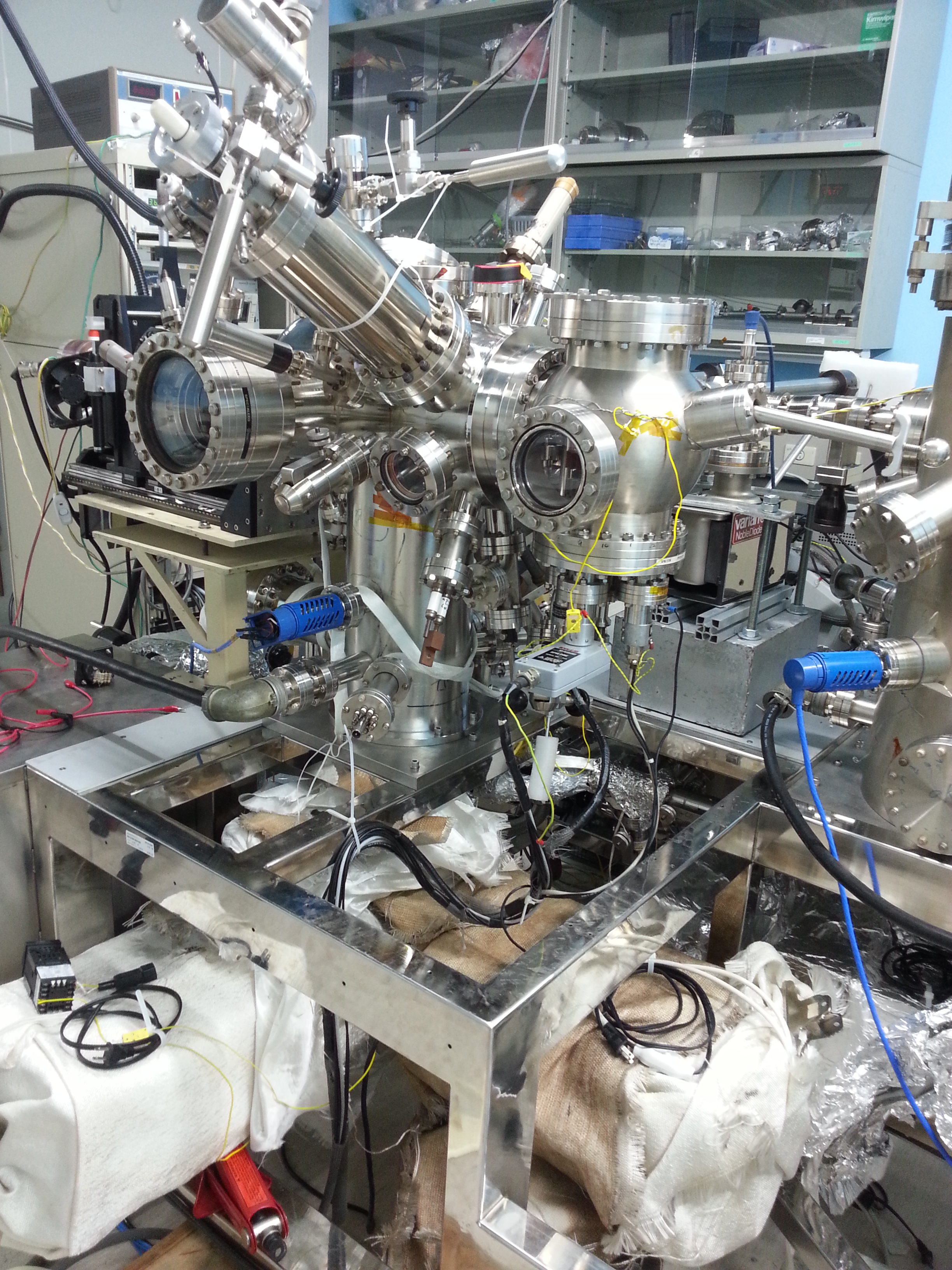
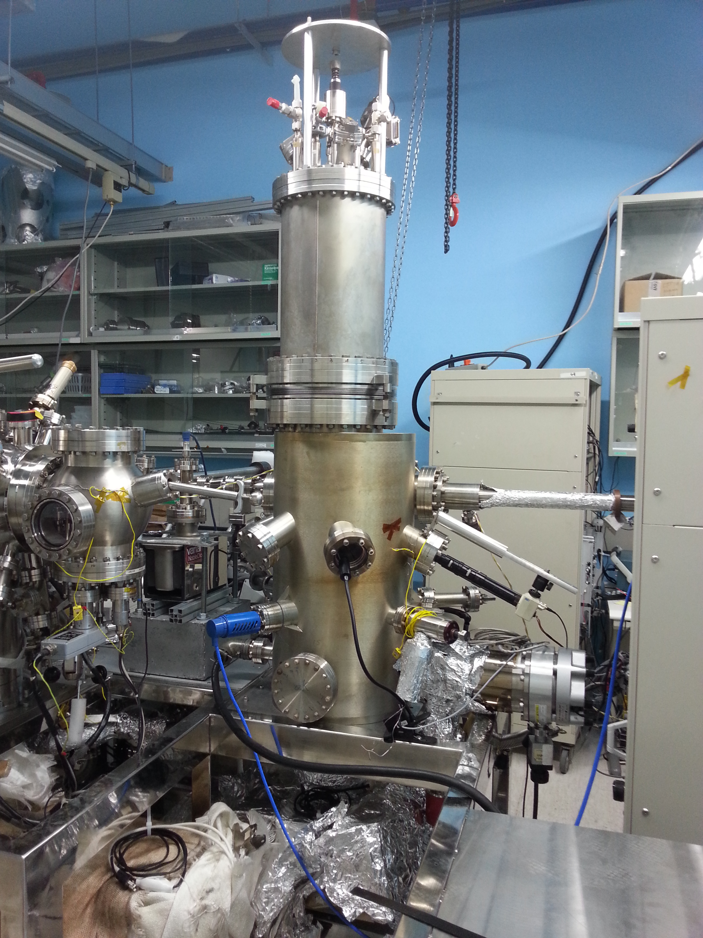
(2) Omicron room temperature STM/AFM system (300 K)
This system can perform scanning tunneling microscopy, non-contact atomic force microscopy and other multi-modes operations. The hosting chamber is equipped with a 4-grid reverse LEED/Auger, K-cell, mini MBE, atomic/ion plasma source, gas train, load lock systems, residual gas analyzer, sample cleaver, 5-degree-freedom manipulator, focused sputtering gun and tip bombard heater, precision sample temperature control etc.
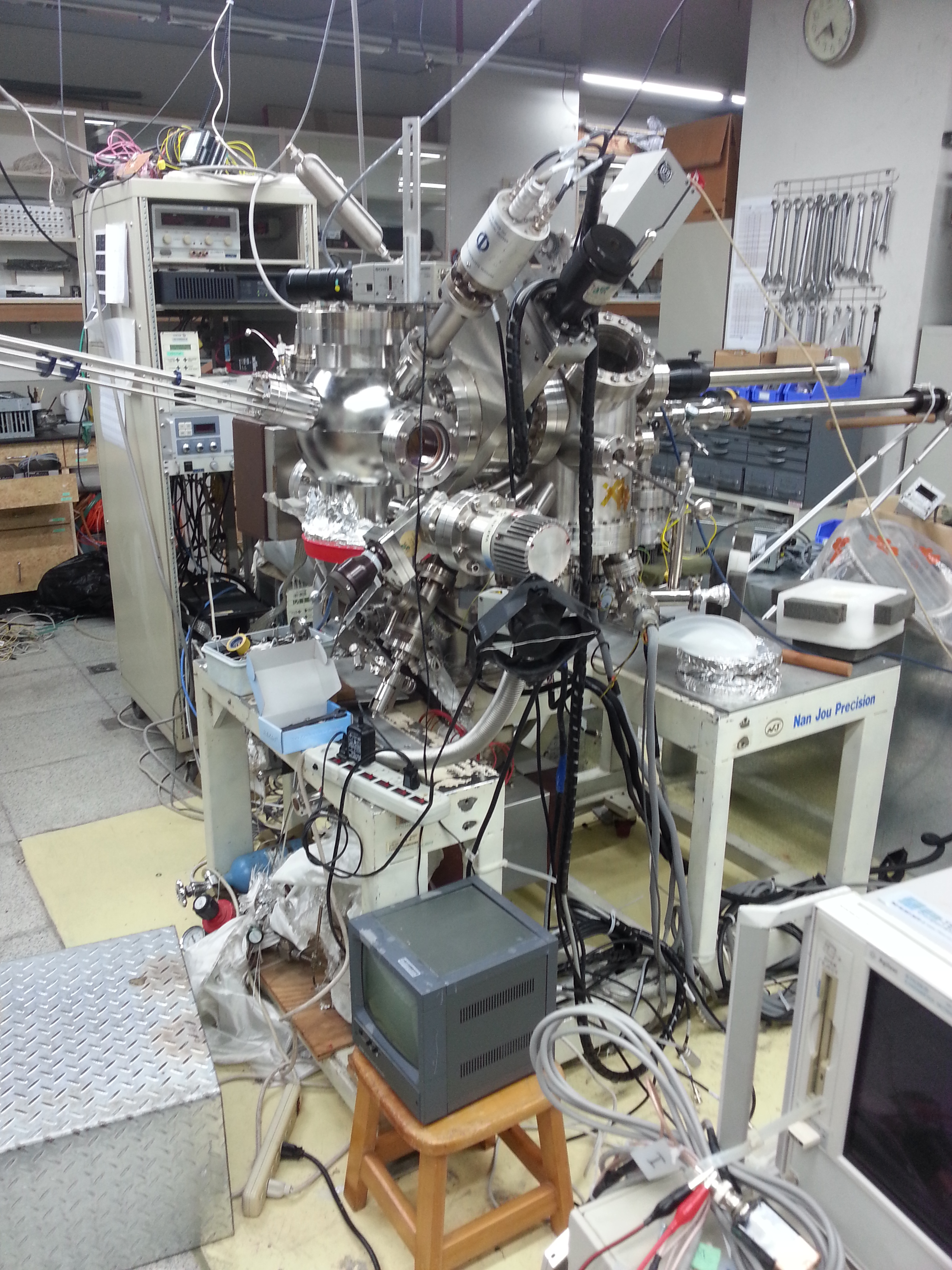
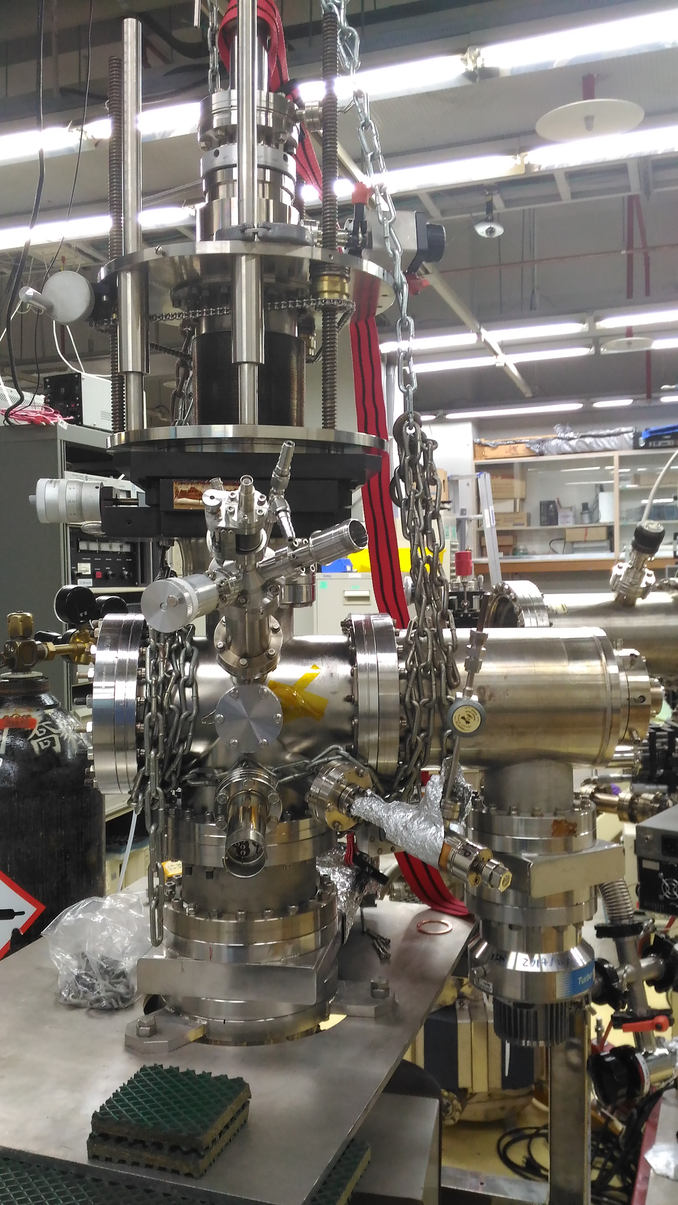
(3) An Omicron low-temperature (4 K, 77K, 300 K) STM/AFM
This system can perform scanning tunneling microscopy, non-contact atomic force microscopy and other multi-modes operations. The system has a base pressure of 3 x 10-11 Torr. It allows detailed atomic microscopic and spectroscopic characterization of materials surfaces and adsorbates. The hosting chamber is equipped with a K-cell, gas line, load lock system, residual gas analyzer, and tip bombard heater. Special optical aid permits characterization of samples in the micron sizes.
In addition, this system is connected to the RT STM/AFM system via load locks. Therefore, samples can be characterized with multiple techniques. Both RT STM/AFM and LTSTM are housed on an enforced stainless steel table with active damping, allowing high resolution characterization.
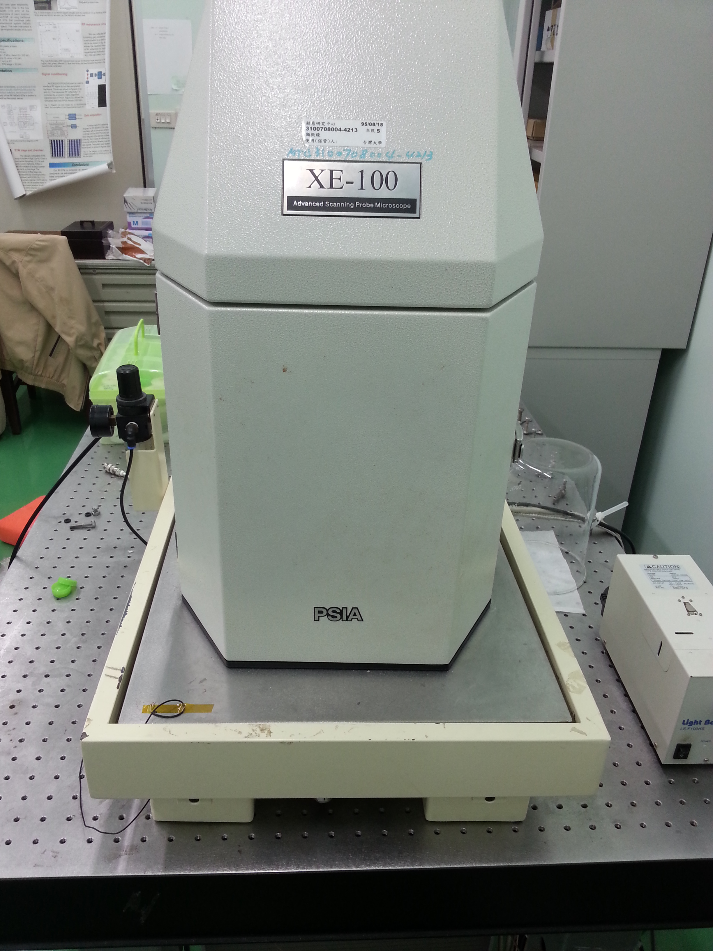
(4) An ambient AFM PSIA (XE-100) system
Additional capabilities to do STM, electric(magnetic) force imaging, and experiments in liquid. This system also provides services to members of all CCMS.
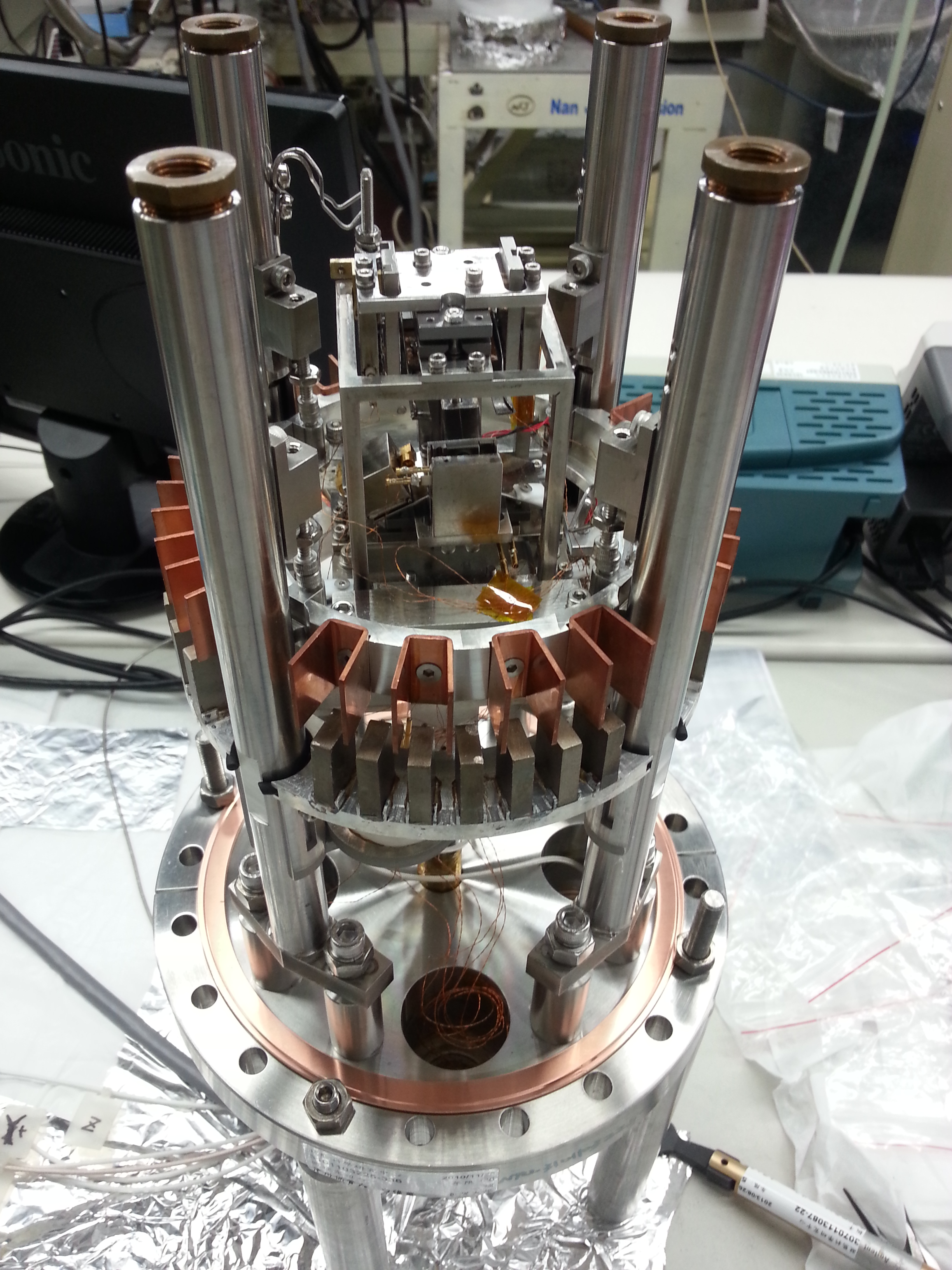
(5) A home-built radio-frequency STM (RFSTM) system.
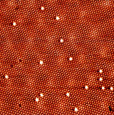
The RFSTM is our patented technique (US patent US8863311). It can achieve a detection bandwidth >500 MHz at a tunneling junction resistance of several hundred mega ohms (a marvelous achievement). It can also detect atomic features on surface in situ with external electron beams or light beams (e.g., X-ray). All parts of the RFSTM are designed and built locally. Special electronics required for RFSTM is also developed and built in our laboratory. The RFSTM version shown below is specially designed to couple to a synchrotron X-ray beam line.
Our RFSTM is capable to observe HOPG atoms and Au surface steps.
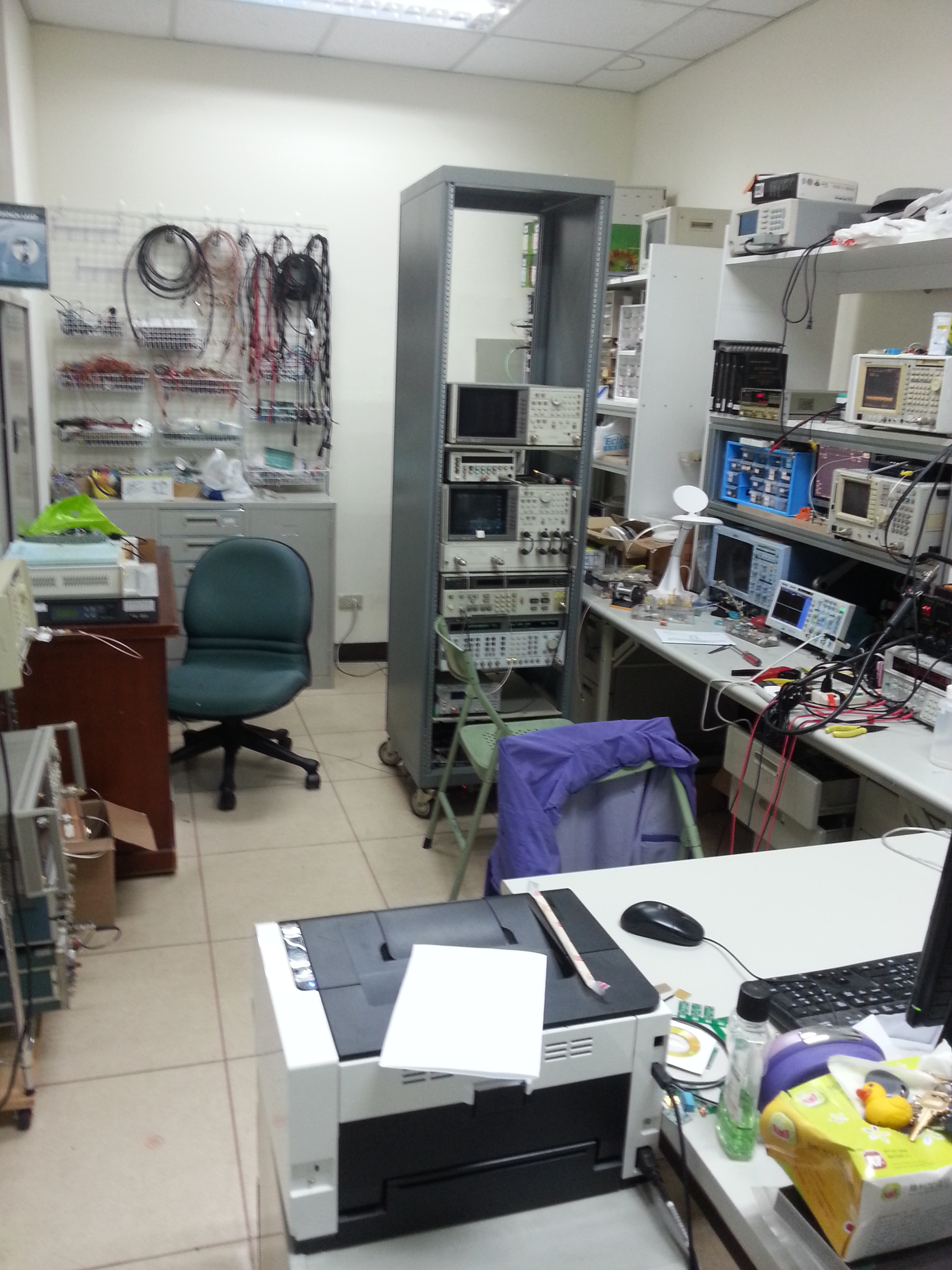
(6) a well-equipped electronic shop for RFSTM development.
Our laboratory also maintains a well-equipped electronic shop, led by an electronics technician of >20 years of experience. Its main purpose is to support the RFSTM electronics. It can also do a wide range of services on electronics.
(7) a temperature programmed desorption (TPD) system
Fast sample temperature control, a Hiden mass analyzer, sample preparation facility. This system is used to study surface reaction and its desorption kinetics.
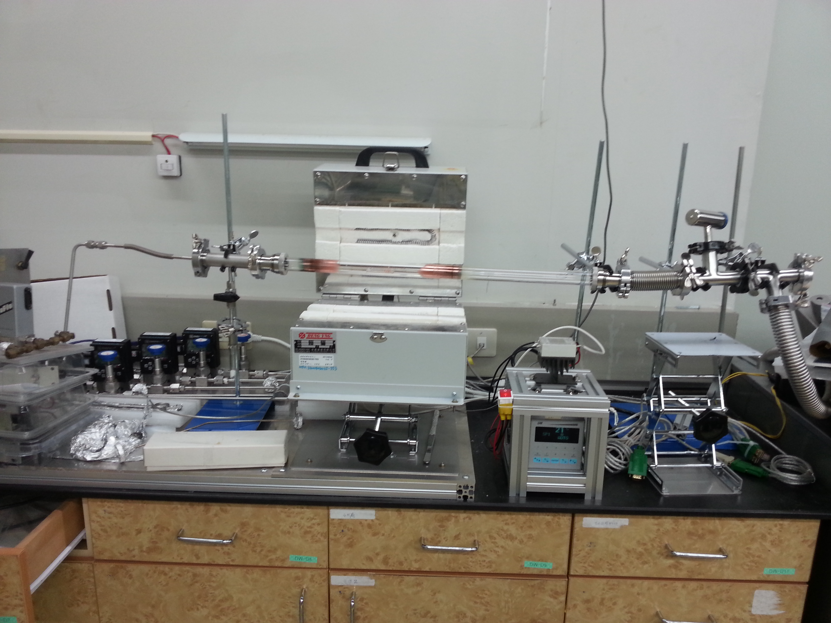
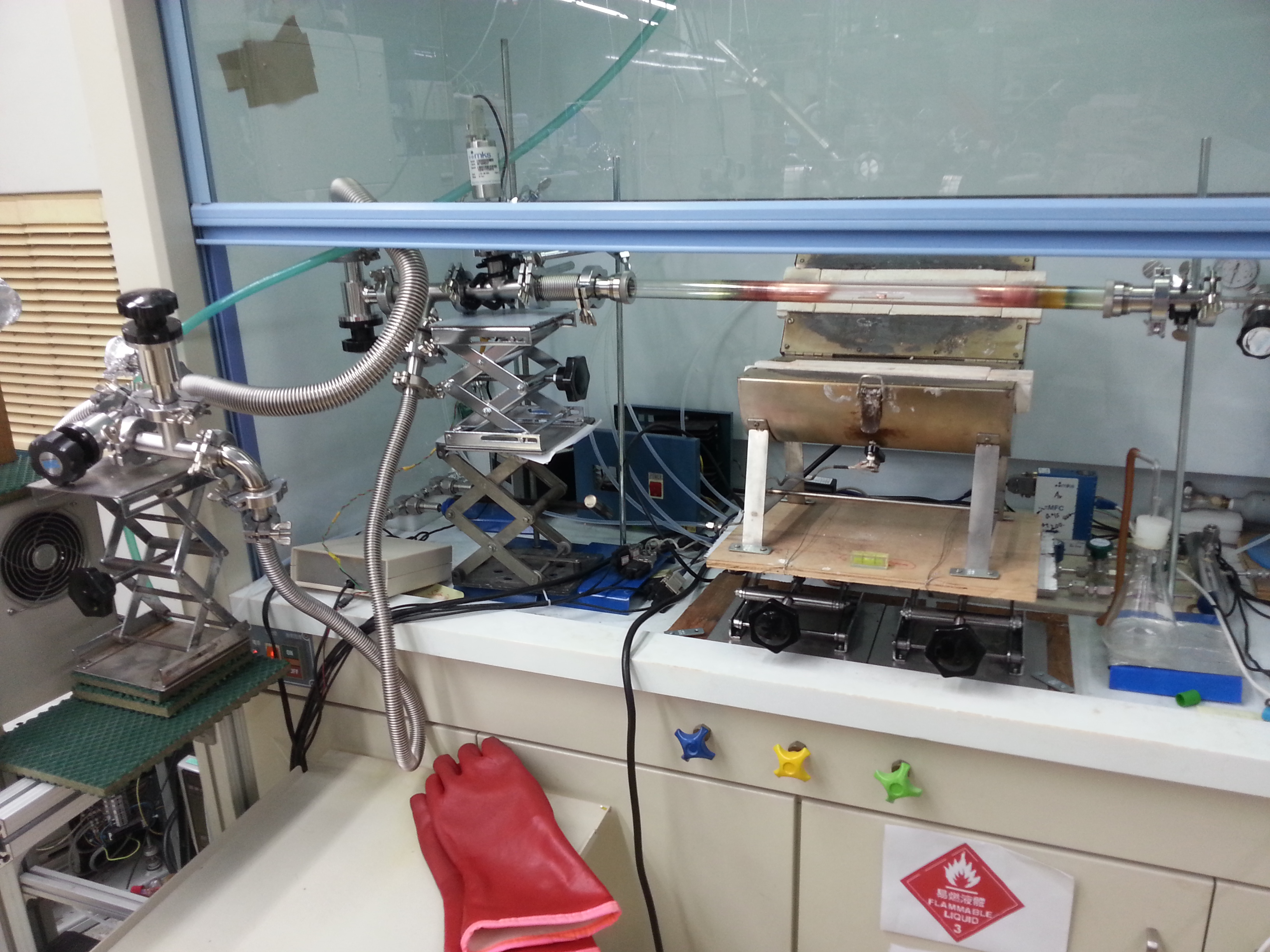
(8) Two home-built chemical vapor deposition (CVD) systems.
The systems are very stable and can grow superior quality functionalized graphene. Other materials (e.g., NbS3) can also be grown by chemical vapor transport in these systems.
(9) Available/Functional but at present unused.
Ibach high-resolution low energy electron energy loss (HR-EELS) system and a general UHV system.