A. Molecular adsorption and structure-property correlations
1. 碳六十分子/金屬介面結構與電荷轉移的關係
Adsorbate-induced properties modification of interface properties
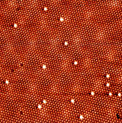
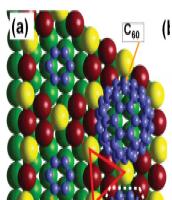
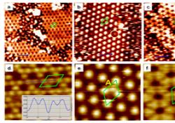
大分子在表面吸附的介面結構是一個相當困難的問題,而介面結構對分子性質的影響就更不容易分析。但這個問題對如分子電子學是極為重要的。在此我們分析碳六十分子在銅(111)表面上介面結構與電荷轉移的關係。我們結合了掃描碳針顯微術與光譜術,光電子能譜,第一原理計算還有低能量電子繞射譜,證明碳六十分子在銅基底上形成了規律的奈米坑(如圖)。特別是,我們發現當有表面重構時,每個碳六十分子得到三個電子,正如碳六十的塊材超導態一般。當表面無重構時,每個碳六十分子得到的電荷轉移就小的多。這是首次發現介面結構可以取代化學摻雜,並造成大量電荷轉移至分子。
2. 透過吸附物調控金屬表面磁性
Adsorbate-induced spin-reorientation transition
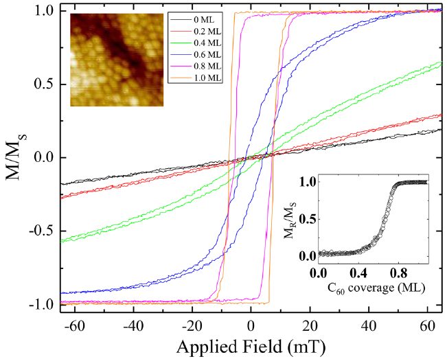
Recently, we also discovered that a C60 overlayer enhances the perpendicular magnetic anisotropy of a C60 thin film on Au(111), inducing an inverse spin reorientation transition from in plane to out of plane. State-of-the-art ab initio calculations shows the underlying mechanism is the local hybridization of C60 pz and Co dz2 orbitals. This opens a way to tailor interfacial magnetic anisotropy in organic-ferromagnet systems.
Ref: “Tuning the Magnetic Anisotropy at a Molecule-Metal Interface”, Phys. Rev. Lett. 114, 247203 (2015)
Raw hysteresis cycles measured during the deposition of C60 on 5.5 ML Co=Aue111T in a polar MOKE configuration.
3. 第一原理計算表面吸附系統
Minimal cluster model of adsorbate-substrate systems
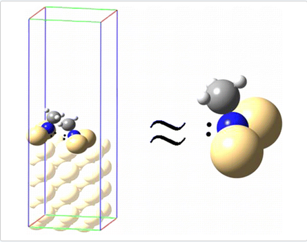
One key aspect of molecular adsorption is how to model the system. One common approach is to use cluster model in which the surface is represented by a sufficiently large cluster with a size not known as a priori. However, if the detailed geometry of surface adsorption is known, the size of representing surface cluster may be significantly reduced. We studied NCH3 adsorbed on Cu(110) and tested the concept of “minimum cluster model”. The whole system is represented by a minimal cluster of NCH3-Cu2, but with its geometry taken directly from periodic DFT rather than optimized cluster geometry. The property of the adsorption system is then analyzed by molecular orbital theory. This combined DFT+MO approach, together with the concept of minimal cluster, yields very good quantitative agreement with experiments for both ground state and excited state properties.
Ref:
“A Minimal Cluster Model of Valence Electrons in Adatom-Assisted Adsorbed Molecules: NCH3/Cu(110) and OCH3/Cu(110)”, J. Phys. Chem. C, 2014, 118 (18), pp 9443–9449 (2014)
“Scanning Tunneling Microscopy and Density Functional Theory Studies of Adatom-Involved Adsorption of Methylnitrene on Copper(110) Surface”, J. Phys. Chem. C, 2013, 117 (23), pp 12111–12116 (2013)
B. 2D or layered materials
1. 黑磷 Black phosphor (Current)
Black phosphor arises as a promising candidate for electronics applications due to its ambipolar conduction and good carrier mobility. One critical issue in BP is its stability in ambient environment, in particular, its interactions with water, oxygen and light. The other issue is BP’s electronic property vs. deformation. We are at present studying the above two issues with high resolution STM. The following is an STM image of the BP surface. We also examine how atomic oxygen atoms interact with the BP surface, and how deformation alters BP’s bandgap.
2. 鈉鈷氧化物表面鈉原子的有序現象
導電鈉鈷氧化物(NaxCoO2, x=0 to 1, sodium cobaltate)是凝態物理領域裡最近熱門的課題之一。這個材料隨著鈉濃度的不同,產生了一系列電性與磁性的相變。其中一項懸而未決的問題是鈉原子的有序現象與材料性質之間的關係。人們一直認為納會帶電荷,其彼此之間的庫倫排斥力會使納原子之間的距離極大化。 我們首次利用掃描穿隧顯微術得到鈉鈷氧化物表面的型態,並且發現表面納原子聚合形成三原子團(trimer) ,並以此三原子團為單元,形成長距有序態。這個發現表明了一個新的有序機制,必須要在了解此材料性質時重新被考慮。
3. 石墨烯:CVD成長及懸浮石墨烯(Current)
Graphene: CVD growth and study of suspended graphene
We have set up two CVD systems for high quality graphene growth. Most interestingly, we found that high quality graphene (with a Hall mobility>2000 Vs/cm2) can form at 300C. There is a synergistic effect of promoted methane activation at the junction of graphene/copper/methane. By monitoring the product gas evolution, we have also determined the activation barrier of this catalytic methane activation.
We also studied how graphene CVD (by methane) is affected by coexistence of biphenyl and naphthalene. Biphenyl has armchair edge and Naphthalene has zigzag edge. We find that Biphenyl promotes graphene CVD growth.
Monolayer graphene is compliant as a membrane yet stronger than steel. Monolayer graphene has been studied in elastic regime but its mechanical properties nearby its presumed pristine rippled state is much less known. By using STM and a Z-V spectroscopy mode, we have studied in great details how a rippled graphene gets deformed. We found a rippled graphene gets flattened out through a series of “flipping” events in which local curvature of graphene becomes reversed. These “flipping” events indicate the presence of metastable monolayer graphene configurations. With a proper control of such metastability, monolayer suspended graphene can be imaged with atomic resolution and is correlated to the process of graphene’s “unrippling”.
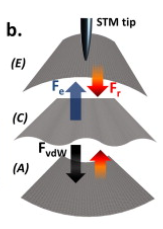
Schematic drawing showing that a suspended graphene can be pulled or pushed to eliminate nanoripples of its pristine state.

STM images showing suspended graphene in pulled-up, pristine, and pushed-down states.
C. 專利儀器開發:射頻STM(Current)
Instrumentation project: Radio-frequency STM
Many types of interactions have been explored in scanning probe microscopies. These include tunneling and various kinds of forces. Another possibility is to sense the tunneling junction impedance by radio frequency wave reflection. The reflection (return loss) depends on the junction impedance ZL. However, useful ZL is typically larger than tens of Mohms, therefore it is difficult to sense such large gap resistance in a standard 50 ohm system.
By using a L-shaped or Pi-shaped tank circuit and treats ZL as a perturbation to the pre-tuned tank circuit, together with a sophisticated vector compensation circuit, we demonstrate radio-frequency STM(RFSTM) can give excellent signal/noise ratio even when ZL > 2 Gohms. We further demonstrate two main benefits of RFSTM: (1) its detection bandwidth is greater than 500 MHz: this is almost 5000 times or more than a conventional transimpedance I-V converter. (2) the RFSTM detection completely decouples from external electric current as high as micro ampere (i.e., e-beam, photoelectrons). Therefore, in situ measurement of electron or photon-induced surface phenomena can be studied readily.
Planned experiments are selective studies of fast surface dynamics (atomic flip-flop), chemical imaging with atomic resolution, and single spin-precession detection.
A home-built RFSTM and its initial test images are shown below.
The 500 MHz detection bandwidth is shown below.
A comparison of atomic resolution in current and RF images (HOPG)
