你好(howdy!)
Recent
publications:
“Radio Frequency Reflectometry
Scanning Tunneling Microscope”, I, J, Chan, H. H. Li,
Woei Wu Pai*,
Taiwan, US
(US88663311) ,German, and China patents granted
Tuning the
magnetic anisotropy at a molecule-metal interface”,
Phys. Rev. Lett.,
24, 247203 (2015).
NbS3: A unique quasi-one-dimensional conductor with three charge
density wave transitions, Phys. Rev. B, 95, 035110 (2017)
Tunable
Se vacancy defects and the unconventional charge density wave in
1T-TiSe2-delta, Phys. Rev. B, 045310 (2017)
Investigating
ultraflexible freestanding graphene by scanning tunneling microscopy
and spectroscopy, Phys. Rev. B, 085433 (2017)
Emergence of charge
density waves and a pseudogap in single-layer TiTe2,
Nature
communication, article number: 8, 516, (2017) DOI:
10.1038/s41467-017-00641
Near room
temperature chemical vapor deposition of graphene with diluted methane
and molten gallium catalyst, Scientific Reports, 7, Artice
No. 12371 (2017)
Dual phase single layer germanene on Ag(111),
Physical review Materials, 2, 024003 (2018)
Characterization of
external potential for field emission resonances and its applications
on nanometer-scale measurements, New Journal of physics, 20, 043014
(2018)
Quantum-spin-Hall insulator with a large gap: single-layer
1T' WSe2, Nature communication,
9(1):2003 (2018)
doi: 10.1038/s41467-018-04395-2
Unique gap structure and symmetry of the charge density wave in
single-layer VSe2, Phys. Rev. Lett.,
121, 196402 (2018)
The basic and
the charge density wave modulated structures of NbS3-II,
Phys. Rev. B, 98, 174113 (2018)
Substrate-mediated umklapp scattering
at the incommensurate interfaces of mono atomic layers.
Phys. Rev. B,
99, 155408 (2019)
Pressure-induced
re-entrant transition in NbS3 phases: combined Raman scattering and
X-ray diffraction study, Phys. Rev. B,
99, 235126 (2019)
Thermoelectric power and its correlation with conductivity in NbS3
whiskers, Phys. Rev. B,
99, 235155 (2019)
Field effect in linear and non-linear conductivity of a layered
quasi-one-dimensional semiconductor TiS3,
JETP 110, 417(2019)
Observing
quantum trapping on MoS2 through the lifetimes of resonant electrons:
revealing the Pauli exclusion principle,
Nanoscale Advances, 2, 5848 (2020)
Germanene structure
enhancement by adjacent insoluble domains of lead, Physical Review
Research, 3 (2021).
The ultra-high-T-P
charge-density wave in the monoclinic phase of NbS3, Journal of
Alloys and Compounds, 854 (2021).
Identification and
Manipulation of Defects in Black Phosphorus, Journal of Physical
Chemistry Letters, 13 (2022) 6276-6282.
Modification of monolayer
1T-VSe2 by selective deposition of vanadium and tellurium, Aip
Advances, 12 (2022).
Formation of Monolayer
Charge Density Waves and Anomalous Edge Doping in Na Doped Bulk
VSe2, Advanced Materials Interfaces, 10 (2023).
This is the Surface NanoScience laboratory in the center for condensed matter sciences at NTU. We do many interesting researches and offer abundant research resources and opportunities. Please visit us!
我們是台大凝態中心表面科學實驗室,我們提供許多資源和機會,看一看這些你有沒有興趣吧!
我們在做什麼?What we do?
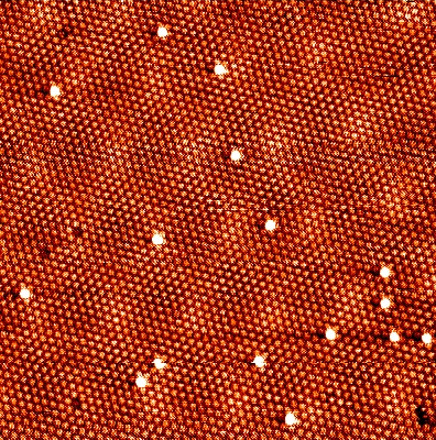
Our laboratory recently focuses on studying 2D and quasi-2D materials, including graphene, black phosphor, ultrathin transition metal dichalcogenides and tri-chalchogenides, and solar cell pervoskites. We use scanning tunneling microscopy/spectroscopy, in combination of other techniques such as ARPES, Raman, TEM etc. and theory to get a better picture of 2D materials properties in atomic and nano scale.
你可以學到什麼?What can you learn?
You will learn sciences in low-dimensional materials, in particular the structure-property correlations in nanoscale.
You will learn many sophisticated experimental techniques, and correct ways of handling these techniques, and a right attitude of doing research.
值得一提的機會?What opportunities?
Besides doing research on topics of your interests, we have many in-house(CCMS), domestic and international collaborations. You are encouraged to probe such opportunities to broaden your horizon.
If you are interested in joining us, please write to Dr. Woei Wu Pai at wpai@ntu.edu.tw
